Copper pour - an area of a PCB layer that is filled with copper. The layer may be the top, bottom or any internal to the PCB stackup and the pour may be used as a ground, reference or to isolate specific components or circuitry from the rest of the elements of the layer.
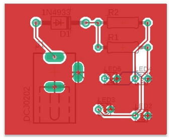
1) The default isolation between the copper layer and the signal traces id "6 mil".
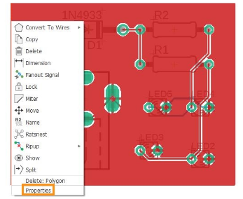
2) To increase the clearance right click on the edge of the polygon and go to properties.
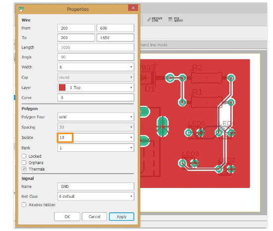
3) In properties, change the isolate value to 10 mil, click "Apply" and then "OK".
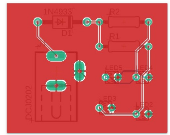
4) The spaces between the copper layer and the signal traces will increase.