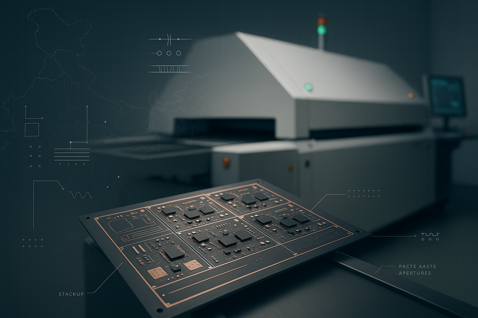
Low noise analog PCB design is a specialized type of printed circuit board (PCB) design that focuses on the accurate and reliable transmission of low-level signals. This type of design is particularly important in applications where noise and interference can compromise the integrity of the signal, such as in sensitive medical or scientific equipment.
The goal of low noise analog PCB design is to minimize the amount of electrical noise that is introduced into the circuit, and to ensure that the signal remains clean and accurate even in the presence of noise and interference. This is achieved through the use of careful component selection, layout, shielding, and filtering and decoupling techniques.
In this article, we will discuss the key principles and techniques of low noise analog PCB design, including component selection, layout, shielding, filtering, and decoupling. We will also provide examples to illustrate these concepts in practice.
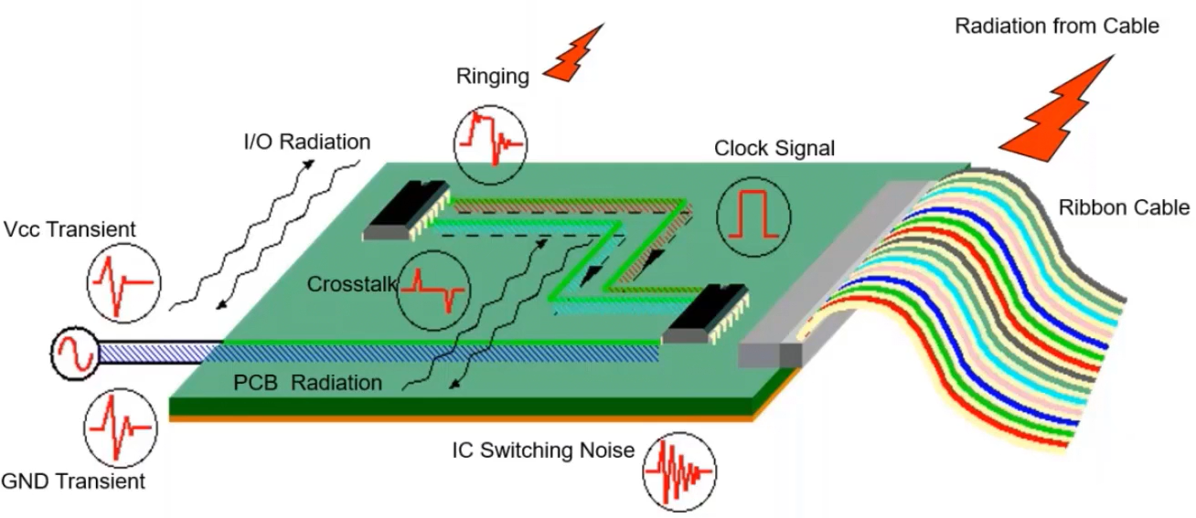
One of the key challenges in low noise analog PCB design is the selection of components. In general, it is best to use low-noise components, such as operational amplifiers (op amps), that have been specifically designed for use in analog circuits. For example, an op amp can be used in a circuit to amplify a weak signal from a sensor, such as a temperature sensor, while minimizing the amount of noise that is introduced into the circuit. It is also important to consider the layout of the components on the PCB, as this can affect the amount of noise that is introduced into the circuit. For example, placing power supply components and sensitive signal-processing components as far away from each other as possible can help to minimize the amount of noise that is introduced into the circuit.
Another important aspect of low noise analog PCB design is the use of shielding. Shielding involves the use of metallic layers or coatings on the PCB to block the entry of external electromagnetic interference (EMI) into the circuit. This can be achieved through the use of grounding layers, as well as the use of shielding cans or enclosures around sensitive components. For example, a PCB used in a medical device might include a metallic layer or coating that acts as a shield, blocking the entry of EMI from external sources such as cell phones or radio transmitters. This can help to ensure that the signals from the medical device remain accurate and reliable, even in environments where there is a high level of EMI present.
In addition to component selection and shielding, the use of filtering and decoupling can also help to reduce noise in low noise analog PCB design. Filtering involves the use of inductors and capacitors to remove unwanted frequencies from the signal, while decoupling involves the use of capacitors to smooth out voltage fluctuations in the power supply. For example, a low pass filter can be used in an analog circuit to remove unwanted high-frequency noise from the signal, while a decoupling capacitor can be used to smooth out voltage fluctuations in the power supply. These techniques can help to improve the signal-to-noise ratio of the circuit, and ensure that the signal remains clean and accurate.
Here are a few examples of low noise design in real world applications:
- Medical equipment: Low noise analog PCB design is crucial in medical equipment, as it allows for the accurate and reliable transmission of signals from sensors and other components. For example, a low noise analog PCB might be used in an electrocardiogram (ECG) machine to accurately measure and transmit the electrical signals produced by the heart.
- Sensors: Low noise analog PCB design is also commonly used in sensors, such as temperature sensors or pressure sensors. In these applications, low noise design is necessary to ensure that the sensor can accurately and reliably measure the desired quantity, even in noisy environments.
- Telecommunications equipment: Low noise analog PCB design is also used in telecommunications equipment, such as radio transmitters and receivers. In these applications, low noise design is necessary to ensure that the signals transmitted by the equipment are clear and accurate, without any interference or distortion.
- Audio equipment: Low noise analog PCB design is also used in audio equipment, such as amplifiers and speakers. In these applications, low noise design is necessary to ensure that the audio signal remains clean and distortion-free, even at high volumes.
- Scientific instruments: Low noise analog PCB design is also used in scientific instruments, such as spectrometers or oscilloscopes. In these applications, low noise design is necessary to ensure that the instrument can accurately and reliably measure the desired quantity, without any interference or distortion.
A step-by-step design walkthrough of a low noise analog temperature sensor PCB.
- Identify the requirements of the circuit: The first step in the design process is to identify the requirements of the temperature sensor. This might include the type of signals that will be transmitted (i.e. temperature readings), the level of noise and interference present in the environment, and the required accuracy and reliability of the signals.
- Select low-noise components: Based on the requirements of the temperature sensor, the next step is to select low-noise components, such as op amps, that are suitable for the application. These components should be specifically designed for use in analog circuits, and should have low levels of noise and distortion.
- Consider the layout of the components: The layout of the components on the PCB is also important in low noise analog PCB design for a temperature sensor. In general, it is best to place power supply components and sensitive signal-processing components as far away from each other as possible, in order to minimize the amount of noise that is introduced into the circuit.
- Use shielding to block external interference: Shielding is another important aspect of low noise analog PCB design for a temperature sensor. This involves the use of metallic layers or coatings on the PCB to block the entry of external electromagnetic interference (EMI) into the circuit. Shielding can be achieved through the use of grounding layers, as well as the use of shielding cans or enclosures around sensitive components.
- Use filtering and decoupling to remove unwanted frequencies and smooth out voltage fluctuations: Filtering and decoupling are additional techniques that can be used to reduce noise in a low noise analog PCB design for a temperature sensor. Filtering involves the use of inductors and capacitors to remove unwanted frequencies from the signal, while decoupling involves the use of capacitors to smooth out voltage fluctuations in the power supply. For example, a low pass filter could be used in the temperature sensor to remove unwanted high-frequency noise from the signal, while a decoupling capacitor could be used to smooth out voltage fluctuations in the power supply. These techniques can help to improve the signal-to-noise ratio of the circuit, and ensure that the temperature readings from the sensor are accurate and reliable.
Overall, the design of a low noise analog PCB for a temperature sensor requires careful consideration of the requirements of the circuit, as well as the use of low-noise components, careful layout, shielding, and filtering and decoupling techniques. By following these principles, it is possible to create a low noise analog PCB for a temperature sensor that is capable of accurately and reliably measuring temperature, even in noisy environments.