


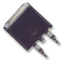
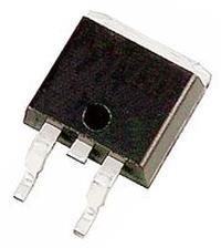

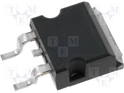
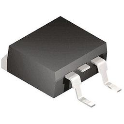


IRF9540NSTRLPBF
Manufacturer
Infineon
Description
Mosfet, Power; P-ch; Vdss -100V; Rds(on) 0.117 Ohm; Id -23A; D2PAK; Pd 110W; Vgs +/-20V
Datasheet
Product Attributes
Type
Case/Package
Contact Plating
Continuous Drain Current (ID)
Drain to Source Breakdown Voltage
Drain to Source Resistance
Drain to Source Voltage (Vdss)
Dual Supply Voltage
Element Configuration
Fall Time
Gate to Source Voltage (Vgs)
Height
Input Capacitance
Lead Free
Length
Lifecycle Status
Max Junction Temperature (Tj)
Max Operating Temperature
Max Power Dissipation
Min Operating Temperature
Mount
Nominal Vgs
Number of Channels
Number of Elements
Number of Pins
On-State Resistance
Package Quantity
Packaging
Power Dissipation
Radiation Hardening
Rds On Max
REACH SVHC
Resistance
Rise Time
RoHS
Schedule B
Termination
Threshold Voltage
Turn-Off Delay Time
Turn-On Delay Time
Width
Description
D2PAK
Tin
-23 A
-100 V
117 mΩ
-100 V
100 V
Single
51 ns
20 V
5.084 mm
1.45 nF
Lead Free
10.668 mm
Production (Last Updated: 4 years ago)
150 °C
150 °C
3.1 W
-55 °C
Surface Mount
4 V
1
1
3
117 mΩ
800
Cut Tape
3.8 W
No
117 mΩ
No
117 mΩ
67 ns
Compliant
8541290080, 8541290080|8541290080, 8541290080|8541290080|8541290080, 8541290080|8541290080|8541290080|8541290080
SMD/SMT
4 V
40 ns
13 ns
9.65 mm
₹221.51
In Stock
Ships in 7-10 days
Quantity
Unit Price
Ext. Price
1
₹221.51
₹221.51
10
₹141.75
₹1417.54
25
₹141.75
₹3543.84
50
₹119.44
₹5972.21
100
₹97.12
₹9712.39
500
₹95.19
₹47593.60
1000
₹65.69
₹65694.26
Product Attributes
Type
Case/Package
Contact Plating
Continuous Drain Current (ID)
Drain to Source Breakdown Voltage
Drain to Source Resistance
Drain to Source Voltage (Vdss)
Dual Supply Voltage
Element Configuration
Fall Time
Gate to Source Voltage (Vgs)
Height
Input Capacitance
Lead Free
Length
Lifecycle Status
Max Junction Temperature (Tj)
Max Operating Temperature
Max Power Dissipation
Min Operating Temperature
Mount
Nominal Vgs
Number of Channels
Number of Elements
Number of Pins
On-State Resistance
Package Quantity
Packaging
Power Dissipation
Radiation Hardening
Rds On Max
REACH SVHC
Resistance
Rise Time
RoHS
Schedule B
Termination
Threshold Voltage
Turn-Off Delay Time
Turn-On Delay Time
Width
Description
D2PAK
Tin
-23 A
-100 V
117 mΩ
-100 V
100 V
Single
51 ns
20 V
5.084 mm
1.45 nF
Lead Free
10.668 mm
Production (Last Updated: 4 years ago)
150 °C
150 °C
3.1 W
-55 °C
Surface Mount
4 V
1
1
3
117 mΩ
800
Cut Tape
3.8 W
No
117 mΩ
No
117 mΩ
67 ns
Compliant
8541290080, 8541290080|8541290080, 8541290080|8541290080|8541290080, 8541290080|8541290080|8541290080|8541290080
SMD/SMT
4 V
40 ns
13 ns
9.65 mm
Other Parts in the same category

prototype to production:
With you at every step
From initial concept to final product, we ensure seamless support at every stage of your manufacturing journey.