Why DFM matters more in India
A board that boots on your lab supply can still choke during fabrication or reflow because of tiny gaps, misaligned layers, or missing test pads. In Indian EMS environments, where machine feeders, stencil house standards, and queue times vary, solid DFM saves you weeks. Think:fewer respins, faster approvals, and cleaner yields. Teams that operationalize DFM see predictable launch cycles and lower total cost of ownership over successive spins.
• Copper-to-edge clearance: Keep ≥ 0.5 mm minimum. Copper too close to the outline risks shorts after routing or enclosure rub.
• Minimum trace/space: Default to ≥ 5/5 mil unless your fab explicitly signs off on tighter. Wider lines and spaces give you more robust etching and yield.
• Annular ring:Size vias for drill wander. Don’t flirt with paper-thin rings; add margin so the finished hole still leaves confident copper.
• Drill table clarity: Spell out plated vs. un-plated holes, the hole sizes, via types (through, micro, blind/buried), and counts to save back-and-forth.
• Material and Tg: If you’re running hot (power, motor control, RF front-ends), callout high-Tg or special laminates and confirm availability early.
.png)
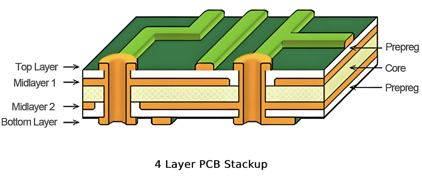
Don’t hand-wave this; document it. Share a full stackup diagram with each layer’s copper weight, dielectric thickness, and material. Mark controlled-impedance nets like USB, HDMI, MIPI, and RF, and list your target ohms and return-path assumptions.
Define width/space pairs per net class using calculations or field solver outputs, and note acceptable tolerance. If your loss budget or flatness matters,specify finish and roughness targets (e.g., ENIG vs. HASL) so the factory doesn’t make unintended substitutions.
Most assembly pain hides here. Keep silkscreen text off pads and out of component keep outs, use legible reference designators, and markpin-1/polarity consistently across footprints.
Allow soldermask tolerance around pads so mask slivers don’t peel or shadow paste.Paste layer accuracy is where bridges and tombstones are born; adjust apertures for very small passives (consider reduced paste or windowing for large thermal pads). Always run your EDA’s DFM/DFXchecks before you export anything.
If pick-and-place has to guess, you lose time and yield. Respect component courtyards so nozzles have room and reflow doesn’t cause part collisions. Use unambiguous polarity symbols for diodes,electrolytics, and IC pin-1; make your footprint silkscreen match the assembly drawing exactly.
Add two or three global fiducials on the panel and local fiducials near fine-pitchBGAs/QFNs so vision systems can align reliably. Keep your BOM and CPLsane: one MPN per line, lifecycle status checked, package fields clean, and rotations/X-Y aligned to the board origin. CPL must match the actual footprints.
Testing isn’t an afterthought; it’s a deliverable. Add test pads or via access for bring-up nets (power rails, reset, clocks,high-risk IO) from the outset. Group test points logically so pogojigs are straightforward and label them in your documentation.
Decide in-circuit test (ICT) versus flying probe early and budget fixture lead time.For firmware-heavy designs, reserve SWD/JTAG/UART headers (mark them DNP if they won’t be populated in production) so you’re never blocked during diagnostics.
A perfect single PCB can still fail in production if the panel is wrong. Add break-off rails to give conveyors and operators something to grip, and to keep parts away from the panel edge. Place consistent 3.0 mm tooling holes in panel corners for fixture alignment.
Choose your breakout method intentionally: V-cut (scoring) yields cleaner edges and is great for straight outlines; mousebites (tabs) handle irregular shapes but require tab keepouts near fragile components. Work with your fab to maximize boards per panel while keeping minimum web widths and tab spacing sane.
.png)
Package your handoff like a pro: a clear fab drawing with notes(board thickness, copper weight, finish, soldermask/silkscreencolors, impedance, and IPC class), a stackup page, Gerbers/ODB++ and drill files, and a netlist if your process uses it.
Your assembly drawing should show placement views for top and bottom, polarity, DNP lists, and any torque or adhesive notes. Keep the BOM clean with primary MPNs and approved alternates, and ensure the CPL aligns with reality, footprints and rotations included. Add a short change log that bullets the deltas from the previous spin so reviewers don’t need to diff files.
Lead-time variance is normal: stencils, special laminates, or exotic finishes can add days. Flag them in your PO notes and request explicit confirmation. If you don’t specify stencil thickness,houses often default to 100–120 µm; dense 0201 designs may need 80–90 µm, say it.
When supply is tight, pre-define approved alternates in the BOM with equivalent specs and the same footprint. Standardizing to 1.6 mm thickness and common soldermask colors can accelerate procurement, especially on quick-turn runs.
• Fabrication notes (thickness, copper weight, finish, color)
• Confirmed stackup with impedance callouts and width/space tables
• DFM-clean silkscreen, soldermask, and paste layers (no slivers; proper apertures)
• Courtyards respected, pin-1/polarity marked, global + local fiducials present
• BOM with MPNs +approved alternates; CPL aligned to footprints and rotations
• Test strategy chosen; grouped test pads; SWD/JTAG/UART access reserved
• Panel drawingwith rails, tooling holes, and breakout details (V-cut or mousebites)
• Gerbers/ODB++ +drill in a versioned ZIP with README + change log
• Special processes (high-Tg, impedance control, finishes) stated and acknowledged
• One point of contact and turnaround expectations documented
Table Of Contents
1) Fabrication rules you should never violate
2) Stackup & impedance: the foundation for signal integrity
3) Silkscreen, soldermask, and paste: tiny layers, huge impact
4) Assembly-ready design: make it machine-friendly
5) Design for test (DFT): test pads now or tears later
6) Panelization: rails, tooling holes, and clean breakout
7) Documentation pack: what “production-ready” actually looks like
8) India-specific gotchas to plan around
9) The ready-to-ship DFM checklist
FAQ
What is DFM for PCBs?
DFM (Design for Manufacturability) shapes your schematic/layout, stackup, and documentation so a real fab/assembly line can build your board at yield and cost, without ad‑hoc fixes.
My prototype worked. Why would production fail?
Production adds tolerances, machine vision, paste dynamics, and panel stresses. A via with minimal annular ring in a one‑off can become an open across hundreds of units.
Do I really need controlled impedance on USB/HDMI?
If you care about signal integrity and EMI, yes. Define target impedances,widths/spaces, and ground references up front.
How many fiducials do I need?
At least two global fiducials on the panel (three preferred) and local fiducials nearfine‑pitch or BGA parts.
V‑cut or mousebites?
V‑cut is ideal for straight edges and cleaner separation; mousebites support irregular shapes but require keepouts near fragile parts and post‑processing for smooth edges.