In today’s fast-growing Indian electronics and PCB manufacturing ecosystem, EMI (Electromagnetic Interference) and EMC (Electromagnetic Compatibility) compliance is no longer optional — it’s essential. Whether you're designing high-speed PCBs, embedded systems, or consumer electronics, understanding how to minimize EMI and pass EMC regulations is crucial for ensuring product reliability, safety, and BIS/TEC certification readiness. From PCB layer stack-up and controlled impedance routing to grounding, shielding, and EMI simulation tools, this guide breaks down practical, India-specific strategies to reduce electromagnetic emissions and noise coupling. Designed for hardware engineers, PCB designers, and electronics startups, this blog will help you master EMI/EMC design principles, avoid costly pre-compliance failures, and meet mandatory Indian standards like IS 13252, IS 14700, and IS 16333. Let’s get your designs EMI-quiet and market-ready.
What is EMI and EMC? (And Why You Should Care)
- EMI, or Electromagnetic Interference, is basically electrical noise. It’s like when one device starts yelling and messes with another one.Think of a speaker buzzing when your phone rings nearby. That’s EMI.
- EMC, or Electromagnetic Compatibility, means your device can do its job without messing with others or getting messed up itself. It’s about being a good neighbor in the electronics world.
Why EMI/EMC Compliance Actually Matters in India:
- India’s electronics industry is growing fast.
- Regulatory bodies like BIS (Bureau of Indian Standards), TEC (Telecommunication Engineering Centre), and MeitY (Ministry of Electronics and Information Technology) strictly enforce EMI/EMC standards.
- Failing EMI/EMC tests = wasted money, lost time, unhappy clients.
Keep in mind: A well-designed board with EMI/EMC in mind usually runs cooler and lasts longer.
Indian EMI/EMC Standards Cheat Sheet:
- IS 13252 (Part 1): ITequipment.
- IS 16333: Telecom EMCcompliance.
- IS 14700 Series: Immunity &emission based on IEC 61000.
EMI/EMCPCB Design Best Practices (The Essentials):
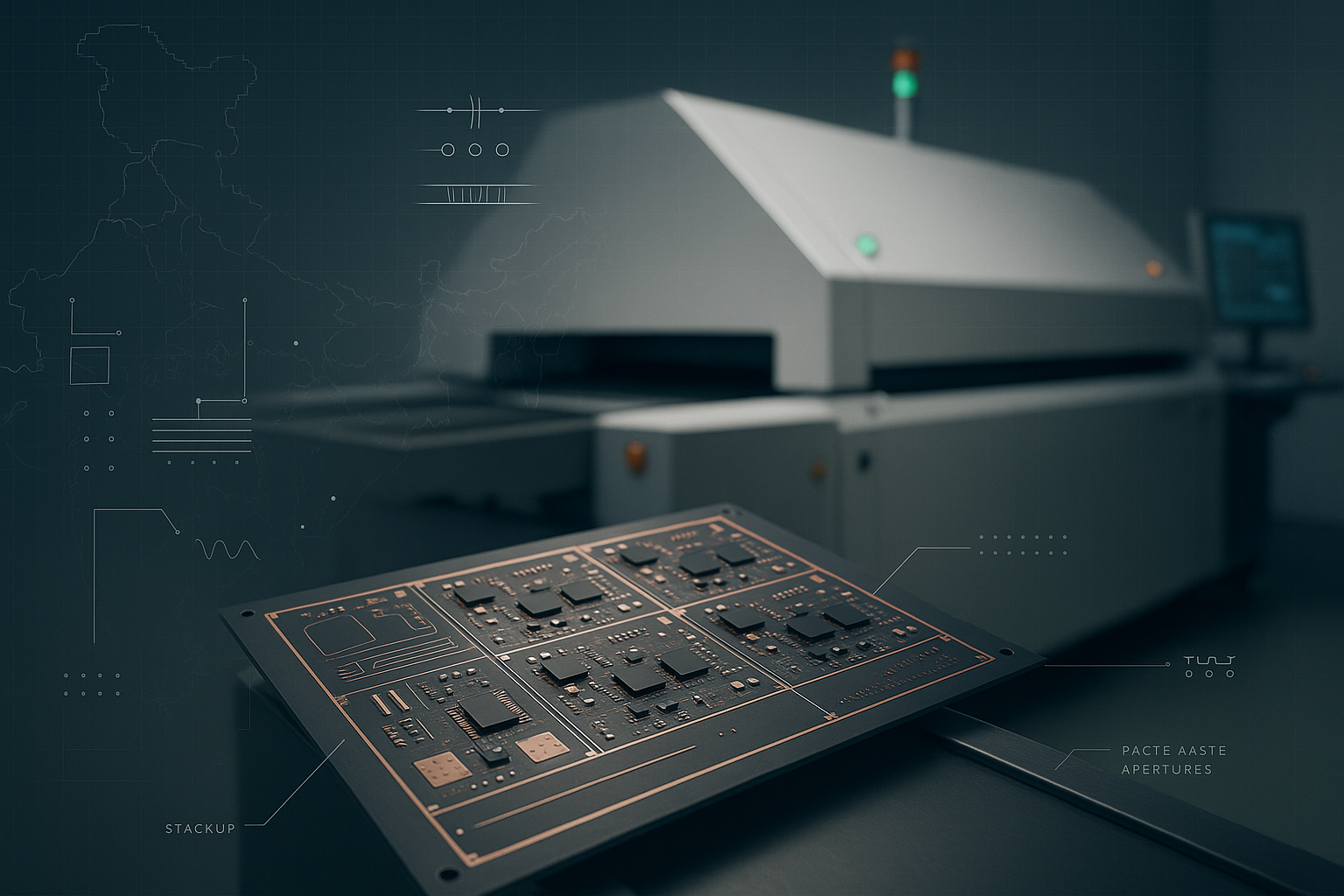
1. Layer Stack-Up:
- Sandwich signal layers between ground and power planes.
- Keeps return paths short and noise contained.
.png)
2. Controlled Impedance = Controlled Chaos:
- Consistent trace width & geometry matters.
- It’s Important for high-speed designs.
3. Smarter Component Placement:
- Keep digital, analog, power sections separate.
- Noisy power circuits stay away from sensitive parts.
.png)
4. Trace Routing Tricks:
- Avoid 90° bends.
- Keep traces short, straight, and inside the board layers.
5. Never forget to add- Decoupling Capacitors:
- Place within 2 mm of IC power pins.
- Not optional at all!
Grounding and Shielding: Your EMI Defense System:
Let’s be honest, most EMI headaches come from poor grounding and shielding. But with a few solid habits, you can lock that noise down.
- Go Solid with Your Ground Plane:
Treat your ground plane like the foundation of a house solid, unbroken, and covering as much area as possible. It gives signals a clean path home and keeps interference at bay.
- Stick to One Grounding Point:
Imagine running extension cords from every corner of your house into a single socket. Chaos, right? That’s what multiple ground points can do. Stick to single-point grounding to avoid nasty ground loops
- Via Stitching? Yes, please:
Add multiple ground vias close together to keep signals clean and reduce EMI.
- Shield Noisy Zones:
Wrap those chatterbox components (like oscillators or switching regulators) in board-level shield like little metal canopies that trap their noise inside.
- Enclose It All:
If you’re using an enclosure, make it conductive and close-fitting with EMI gaskets. And do not forget your cable. shield them and ground those shields properly (at one end!).
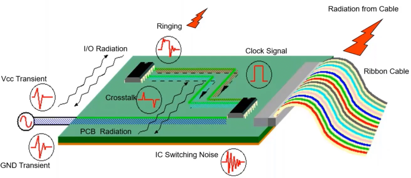
How to Kill Radiated and Conducted Emissions:
Ever seen your PCB behaving weirdly and wondered why? That’s often because high-speed signals are sneaking out as uninvited radio waves.
How to Keep It in Check:
- Move those sensitive traces to inner layers: - hide them.
- Leave some breathing room at least 6mm from the PCB.
- Keep loops small: - tight paths mean less noise.
- Run a quick EMI simulation before sending your design to the manufacturing.
Pre-Compliance Testing: Don’t Skip It:
What You’ll Need:
- A Spectrum Analyzer with an Antenna to check for signal leaks.
- LISN(Line Impedance Stabilization Network) to test power line noise.
- Signal Generators to simulate real-world interference.
Common Mistakes PCB Designers Make (And How to Dodge Them)
Even pros miss these sometimes. Here’s what usually goes wrong and how to handle it:
- Split Ground Planes: Always use one solid ground plane: -no gaps.
- Messy Layout: Keep analog, digital, and power zones separate.
- Forgetting EMI Early: Plan for EMI from the first step, not as an afterthought.
- No Cable Shielding: Use shielded cables where needed to avoid unwanted noise.
Quick EMI/EMC Compliance Checklist
Before you send your design off to manufacturing, quickly check these essentials:
- Continuous ground/power planes?
- No 90° bends?
- Decoupling capacitors close to ICs?
- Shields for cables and enclosures?
- Pre-compliance testing complete?
- Indian BIS/TEC rules checked?
When in doubt:
Achieve EMI/EMC compliance effortlessly with expert PCB design support from LionCircuits.
References:
- Bureau of Indian Standards. “IS 13252 (Part 1): Safety of Information Technology Equipment.” BIS, 2010
- Ministry of Electronics & IT. “EMI/EMC Testing Guidelines.” MeitY, 2024.STQC Directorate. “EMI/EMC Testing Capabilities.” Government of India, 2025
- Texas Instruments. “PCB Design Guidelines for Reduced EMI.” Application Report SLVA631, 2014.
- Altium Resources. “PCB Noise Reduction Through Signal Isolation.”Altium, 2023.