In this article, We will dive deep into Track Impedance and Placement in High-Speed Hardware Layout Design. Click to read PART-1 and PART-2. Let’s continue from where we left.
Track Impedance:
Impedance is the effective resistance (literally) to the flow of current. It is a combination of both the power dissipating resistive load and a reactive load (reactance, causing a reactive power loss). Impedance matching is paramount in any high-speed design!
It would be amusing to know that components like capacitors, inductors or resistors are not the only components that have capacitance, inductance or resistance. The truth is that every real-world component that you place on a board or even a PCB trace have these basic 3 parasitic elements (capacitor, inductor or resistor) embedded at some part of their system. It may be in such low orders of magnitude that we tend to ignore them most of the time and move on with our lives as circuit designers. Well, until we hit move to designing high speed/or a high power dense board. This is where we realize that these small parasitic in the order of Nano or even Pico can create reactive voltage spikes which can damage your puny driver, or perhaps cause your favorite communication protocols to talk utter gibberish.
The theory behind impedance matching is simple and can be explained in more than one way. In one sentence the RF engineers have gotten the idea correct. Maximum power transfer takes place when impedances of both the source and load are matched! To match impedances, you have to:
- Match the Lengths of tracks (that have differential signaling) on each layer.
- Send your layer stack up to your manufacturer and get your trace width for the impedance for each layer.
- Now, use that track width and spacing on each layer!
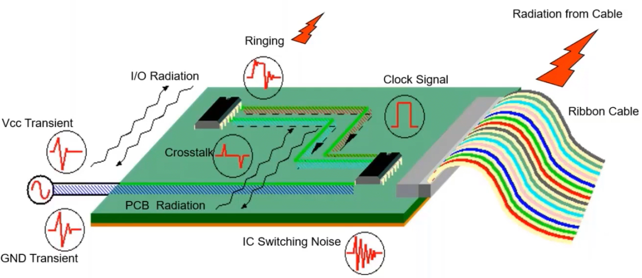
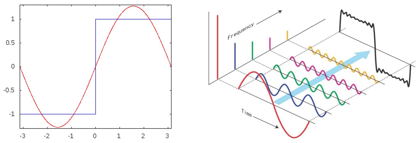
To further improve your SI, you can terminate your signals. Some low-speed signals such as a UART, etc. are terminated by using a series resistor, this is not done to match impedances but rather to reduce the rise and fall time. Sharp transitions are the leading cause of EMI in a system and not the frequency at which the communication protocol is communicating (as some assume it to be). This is because sharp transitions are formed by the combinations of frequencies across a spectrum. Unless your system is communicating in sine waves, you are bound to see a wide spectrum of frequencies in your signal, this is because any signal can be deconstructed into a series of sine waves and a square wave is a combination of an infinite number of sine waves!
You can estimate the bandwidth of frequencies in a square wave using the formulae below:
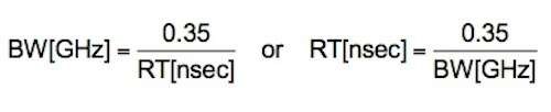
Where:
RT = the 10-90% rise time of a square wave in nsec
BW = the bandwidth of the signal, in GHz
More on Bandwidth can be found here.
Placement:
Now we have discussed earlier that proper placement of components is key to maintaining a good SI and EMI/EMC. This largely due to the fact that longer return loops act as antennas and radiate. This affects the SI of your system and also your system up for failure in EMC tests. To improve your layout additionally, there are just two more points you can keep in mind, Keep your tracks as short as possible (keeping inductance in check) and keep your return path on an uncut solid ground plane (keeping capacitive coupling in check).
To keep your inductance low, terminate your system traces as quickly and short as possible. Do not use stubs anywhere and make your tracks as wide as possible to reduce inductance. When talking about Intra-board EMI in high speed and low current systems. The word interference mostly is attributed to capacitive (electric fields) coupling. Electric field EMI are easier to tackle because they are generated with a set two oppositely charged tracks that have a relative potential difference across them (like the two plates of a capacitor) and containing the field is as easy as making your own PCB sandwich capacitor with the track on one side and the GND on the other side, which also how return currents are channeled.
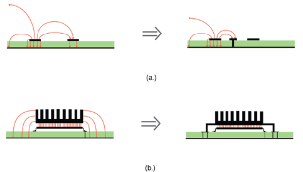
Via’s have inherent inductance and also self-resonance frequencies, which have to have to be taken into consideration when routing High-Speed traces. Its good minimize the amount of via’s on these traces as much as possible. If you have added a via to a differential pair make sure you have it in all the traces that are within the same group so that the impedance and timings are matched. This helps maintain the timing skew and make sure that all the signals reach within the latching window.
To keep your return path as predictable and as short as possible. Keep and uncut reference plane as close to the layer as possible in the high-speed design and always consider your return current paths in low-speed designs. The capacitive impedance decreases allowing a considerable amount of return current to the couple through anything that is capacitively coupled (like for your traces underneath your high-speed tracks). Here’s where things get interesting, increasing frequency makes capacitive impedance to drastically reduce, this means that your signals are returning more and more through the captivity that is formed than along the resistive path back to the chip (only in high signals).
The placement of your system should be done with the digital section of the board physically placed away from the analog section of the board. The board layout designer must ensure that there will be no interference both through the boards and air (can happen in mother-board configuration) into the analog section. Having a solid ground plane is still the best approach even if you’re routing a system with a high-speed DDR3 ram on the same board. This is only possible after taking care of the fact the board is properly placed and now digital currents can return without going into the analog ground section.
The conventional understanding of circuit design is stretched when the propagation of a high-speed signal is considered as a movement of electrons on the board. It finds it hard to explain SI or even something as simple as what is the characteristic impedance of a wire. A great book on this is Ralph Morrison’s Fast Circuit Boards: Energy Management, which looks more like a book authored by a physicist than a veteran form the electronics design community. Ralph Morrison has been in the game of high-speed design for all of his career. And this book is a splendid outcome of that solid experience. When you reach the GHz range you are neck deep in the high-speed territory. And this movement of signals can be best explained by what he calls “energy management”. It breaks down the conventional understanding that signals are a product of the movement of electrons from one point to another. Here Ralph makes a point that what high-speed engineers do is nothing short of “energy management” of signals moving from one section of the board to another.
This fundamental view in electronics design is now revolutionizing how we look at EMC/EMI in the 21st Century and how high-speed designs are done in the industry. Having a strict rule-based design with considerations for proper energy management can help you design systems as complex as processors with multiple DDR3 interfaces to work and pass EMC compliance tests with flying colors, and that too without the help of a single simulation.
.png)
About the Author:
Tony is currently the Lead Hardware Design Engineer at Nymble Labs, Bangalore, India. He is a conventional electronics geek and love to indulge in anything and everything related to chips (fried and baked alike!). His experience mainly revolves around Mixed-signal design and Power electronics with a dab of High-Speed Design and EMC/EMI. In the meanwhile, he reads books and listens to podcasts that center around history and human psychology as a diversion. He often loves to geek out, and making a conversation with him is so much easier when it’s on any one of these topics.